
We have evaluated some of the most recent breakthroughs in the synthesis and applications of graphene and graphene-based nanomaterials. This review includes three major categories. The first section consists of an overview of the structure and properties, including thermal, optical, and electrical transport. Recent developments in the synthesis techniques are elaborated in the second section. A number of top–down strategies for the synthesis of graphene, including exfoliation and chemical reduction of graphene oxide, are discussed. A few bottom–up synthesis methods for graphene are also covered, including thermal chemical vapor deposition, plasma-enhanced chemical vapor deposition, thermal decomposition of silicon, unzipping of carbon nanotubes, and others. The final section provides the recent innovations in graphene applications and the commercial availability of graphene-based devices.
Avoid common mistakes on your manuscript.
In 2004, Geim et al. synthesized a stable monolayer of graphene through mechanical stripping. Geim and Novoselov were awarded the Nobel Prize in Physics in 2010 for their successful experiments, and, subsequently, graphene became one of the world's most studied two-dimensional materials. 1 Graphene is a single atomic layer of carbon atoms arranged in a hexagonal pattern. It has a thickness of only 0.334 nm, making it the world's thinnest material. It has numerous distinguishing qualities due to its unique properties, such as a large specific surface area (~ 2600 m 2 /g), 1 high electron mobility (200,000 cm 2 /Vs), 2 enhanced thermal conductivity (3000–5000 Wm/K), 3 extreme optical transparency (97.4%), 4 and exceptional mechanical strength, with a Young’s modulus of 1 TPa. 5
An experimental demonstration of the thermal chemical vapor deposition (CVD) method for synthesizing a few-layer nano-graphene with roughly 35 layers of graphene was made 2 years after the first report on graphene synthesis. 6 To create a large-area graphitic film with three to six graphene layers, Obraztsov et al. resorted to the CVD approach. 7 Eda et al. produced large-area (10 cm 2 ) reduced graphene oxide (rGO) film using the vacuum infiltration method. 8 In 2009, Li et al. used the CVD approach to successfully create high-quality, large-area uniform graphene sheets on copper substrates. 9 In their study, more than 95% of the 1-cm 2 film was monolayer graphene, 3–4% was bilayer graphene (BLG), and the remaining 1% was few-layer graphene (FLG). They discovered that graphene formed on copper via a surface-catalyzed mechanism. They also demonstrated graphene synthesis on a quartz substrate with an improved approach for transferring graphene to other substrates with minimum defects. Bae et al. reported the first roll-to-roll (R2R) method for producing large-`area 30-inch (c. 760 mm) diagonal films utilizing CVD on flexible ultra-large copper substrates. 10 With the R2R approach, the films can be transferred directly onto the desired substrate. Paton et al. synthesized graphene nanoplatelets (GNP) from graphite by liquid phase exfoliations (LPE) in 2014. 11 The GNPs produced by LPE have a limited lateral dimension of a few micrometers, and can range in thickness from monolayer to more than ten layers. Later, Luong et al. established flash Joule heating as a quick, effective, and scalable method to produce graphene in a few grams from a range of feedstocks, including waste food, plastics, coal, carbon black, and petroleum coke. 12 This was the breakthrough research in the direction of graphene commercialization. The technique employs a "flash" of electricity to heat the carbon to approximately 3000 K, converting it into graphene flakes.
Graphene’s high electron mobility makes it an ideal material for semiconductor device applications requiring fast response times. 13,14 The high conductivity of graphene combined with high optical transparency has attracted applications such as a transparent conductive layer for photonic devices. 15 In addition to these, graphene holds a great deal of promise for other areas, such as anticorrosion coatings 16 and paints, 17 sensors, 17 wearable and flexible displays, 18 solar panels, 19 faster DNA sequencing, 20 drug delivery, 21 etc. Most of these applications require high-quality SLG or BLG. The last few years have seen much progress in the controllable synthesis and large-scale synthesis of graphene by mechanical exfoliation 22 or chemical exfoliation, 23 as well as CVD. 24,25 The production methods and subsequent processing techniques mostly decide the morphology and structure of the graphene, and also govern the potential applications. Therefore, Sect. 2 reports on the structure and properties, while Sect. 3 covers synthesis techniques, followed by a detailed discussion of its potential applications.
The number of layers of graphene regulates the different properties. SLG and BLG are zero band gap semiconductors owing to the encounter of the conduction and the valance bands at the Dirac points. 26 A band gap can be opened in BLG by the application of an electric field. 27 Furthermore, for FLG, the structure becomes more metallic with increasing layers. 28 Hence, to comprehend the application of graphene, it is crucial to first understand the graphene properties. This section will review the structure and properties of graphene.
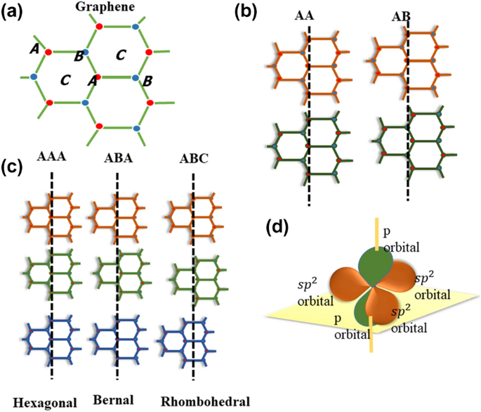
SLG is a sp 2 hybridized structure with two carbon atoms in a unit cell, and these two carbon atoms are located in the A and B positions, respectively (Fig. 1a). 29 BLG can be divided primarily into three categories: AA-stacked, AB-stacked, and twisted 29,30 (Fig. 1b). On the other hand, tri-layer graphene (TLG) has three stacking options. The AAA, ABA, and ABC stacking sequences represent the hexagonal, Bernal, and rhombohedral arrangements, respectively 31 (Fig. 1c). Three out of four valence electrons for each carbon atom in graphene's honeycomb lattice overlap with the adjacent carbon atom within the sheet, forming a strong sigma bond. The exceptional flexibility and robustness of graphene's lattice structure are due to the sigma bond. The remaining fourth electron in the Pz orbital overlaps with the neighboring orbitals and forms a π bond that regulates the interaction between the graphene layers (Fig. 1d).
Two linear bands in the band structure of the SLG cross at the Fermi level in the first Brillouin zone, which are Dirac points. Graphene is thus a zero-gap semiconductor (Fig. 2a). 27 Holes and electrons near the Dirac point behave as massless fermions (m* = 0) and travel at extremely high speeds (10 6 m/s). SLG is recognized as a crucial material for electronics devices due to its outstanding properties and high flexibility. However, the zero-gap constrains its applications. Hence, the first obstacle to overcome is the opening of a gap. A perpendicular electric field applied across the graphene layer tunes the band gap of BLG and TLG due to different stacking sequences. 30,31 Oostinga et al. demonstrated the change in carrier mobility from ∼ 1,000 cm 2 /Vs to ∼ 3,000 cm 2 /Vs by tuning the gate voltage 27 (Fig. 2b–c).
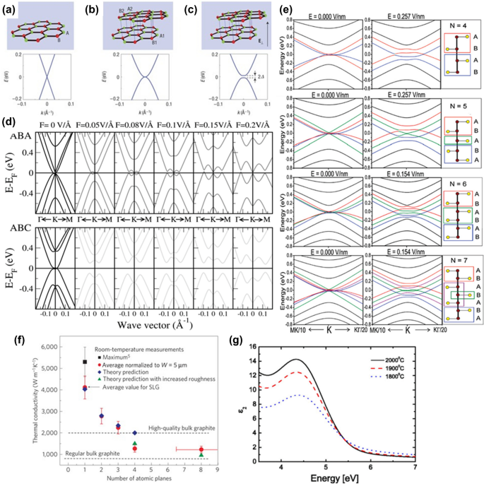
In the low-energy region, Bernal TLG has two parabolic bands and one pair of linear bands, as shown in Fig. 2d. 32 When the electric field exceeds 1 V/nm, the top of the valence band exceeds the bottom of the conduction band, and the band gap disappears. The energy gap of Bernal BLG varies monotonically with the electric field. Thus, Bernal TLG behaves like a semimetal in the perpendicular electric field. Near the K point, there are three pairs of parabolic bands for the rhombohedral TLG. When the perpendicular electric field is continuously increased, the energy gap for initially increases and then decreases. Bernal and rhombohedral TLG have different electronic properties due to stacking sequences.
FLG’s electronic structure is extremely sensitive to thickness, becoming increasingly metallic with increasing layers. Tang et al. investigated the effects of an electric field on FLG with layer numbers greater than 4. 33 An external electric field can convert all ABC stacking graphene with N > 4 to semiconductors, whereas ABA stacking graphene remains semi-metallic (Fig. 2e).
In addition to its distinctive electrical properties, graphene has a very high thermal conductivity. At ambient temperature, the intrinsic thermal conductivity of single-layer suspended graphene is in the range of 4800–5300 W/mK 4 . In comparison, high-quality graphite has a thermal conductivity of only 2000 W/mK. Suspended graphene from CVD has a thermal conductivity that ranges from 1500 to 5000 W/mK at room temperature (RT). 36 A number of independent experimental reports have validated graphene's high thermal conductivity values. 37,38,39,40 The thermal conductivity of supported graphene at RT is 600 W/mK and is lower than that of suspended graphene due to phonon scattering at the defects site and thermal coupling to the substrate. 41 Graphene flake thermal conductivity changes with size, and that heat is transferred mainly by acoustic phonons. For instance, the thermal conductivity of suspended FLG initially reduces with an increasing number of layers, then recovers and reaches the bulk graphite limit of 2000 W/mK (Fig. 2f). 34 The intrinsic features defined by phonon–phonon scattering help to address the interdependence of thermal conductivities on the number of graphene layers. As the number of graphene layers increases, the phonon dispersion changes, resulting in more phonon states available for Umklapp scattering. The greater the Umklapp scattering, the lower the inherent thermal conductivity.
Graphene's unique optical feature can be attributed to its distinctive two-dimensional band structure. 42 It has been shown from the linear optical characterization that graphene absorbs approximately 2.3% of the incident red light and 2.6% of the green light. 43 However, the relationship is linear, and each layer absorbs 2.3% of light. This means that a graphene sample with 5 layers would absorb 11.5% of light and be about 88% transparent. 44 In addition, graphene absorbs over a wide spectral range, from the visible to the infrared region. 45 Interband transitions could explain the light absorption from the visible to the near-infrared range. On the other hand, intraband transitions or free carrier absorption are responsible for the optical response in the far infrared range. As graphene lacks definite energy band levels, it can absorb the radiation regardless of its frequency. Graphene may also produce optical transitions in electric fields, known as gate-dependent optical transitions. 46 The low density of states at the Dirac point causes the Fermi level of graphene to change in the presence of an applied electrical field. This property is useful in electronics to modulate the current, because a change in the Fermi level modifies conductivity, as well as tunes the transmission of an optical source. Ni et al. obtained the refractive index (n) of monolayer graphene grown on a 285-nm-thick Si substrate as n = 2.0 − 1.1i in the visible spectrum, slightly different from that of bulk graphite, nG = 2.6 − 1.3i. 47 The refractive index of graphene on such substrates depends on the wavelength and the incident angle of the illumination. By fitting to experimental spectra as a function of wavelength, the complex refractive index of graphene and graphite may be generally represented as n = 3 − iC/(3λ) (where λ is wavelength and C = 5.446 μm −1 ). 48 Ochoa-Martínez et al. reported the refractive index of monolayer graphene as ~ 4 and for bilayer graphene as ~ 3.5. 49 A dielectric function is the sum of real and imaginary dielectric functions. 50 The graph between imaginary dielectric function and critical point (CP) transition energy is used to deduce the thickness dependence of the graphene on dielectric function. Bouhafs et al. reported that the dielectric function of graphene increases as the number of graphene layers grows, or as the temperature of graphene growth increases (Fig. 2g). 35 While graphene synthesized at 2000°C exhibits a dielectric function comparable to that of graphite, graphene formed at 1800°C exhibits graphene-like characteristics. The CP transition energy in the dielectric function of graphene is red-shifted with increasing thickness (or temperature), which is accompanied by an increase in polarizability, as shown in Fig. 2. Exceptionally higher mechanical properties of graphene have been assessed using an atomic force microscope, and the intrinsic breaking strength and elasticity of free-standing monolayer graphene are reported as 130 GPa and 1 TPa, respectively 51,52 Table I shows the comparison between some properties of SLG, BLG, FLG, GO, and rGO.
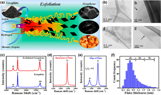
One of the traditional techniques for producing large amounts of graphene is the chemical reduction of GO. Initially, GO is produced via graphite oxidation using the modified Hummers method. 84 Then, the prepared GO is reduced by hydrazine 85 and sodium borohydride. 86 The chemical reducing agents like hydrazine are not environmentally friendly and create hazardous by-products. 87 Hence, researchers started to find safe and environmentally friendly reducing agents. 88
Abdolhosseinzadeh et al. reported fully scalable graphene mass production by reducing graphite oxide with ascorbic acid. 89 A different approach is with plant-based extracts being used as a reducing agent, as these are non-hazardous, comparatively cheap, and easily available in the market. Upadhyay et al. used grape extract as an alternative to the conventional toxic reducing agents. 90 Mahata et al. have used Tulsi leaf as a green alternative for bio-reduction of GO with 90% yield. 91 In a recent review, Park et al. reported detailed information about the chemical methods for graphene production. 92
In the CVD method, gas species are brought into the reactor, where they travel through the hot zone. At the surface of the metal substrate, hydrocarbon precursors break down into carbon radicals. These carbon radicals then self-assemble to form the graphene layer. In the course of the reaction, the metal substrate acts as a catalyst and affects the quality of graphene. In recent years, a variety of transition metals, such as Ru, 93 Ir, 94 Pt, 95,96 Co, 97 Pd, 98 Ni, 99 and Cu, 100,101,102 have been used as a catalyst.
The solubility of carbon in Cu is 0.04% at 1000°C. 103 The graphene growth happens via surface adsorption in Cu due to low solubility, while surface segregation/precipitation is the main mechanism in metals such as Ni having higher solubility. Therefore, it is easier to obtain a monolayer graphene on a Cu substrate. Wood et al. reported growing mono- to few-layer graphene on polycrystalline Cu at 1000°C using methane (CH4). The crystal quality and the orientation of the Cu substrate greatly influenced the quality of the graphene growth. After CVD, Raman spectroscopy shows that the (111) having facets produce pristine monolayer graphene while Cu (100) surface prefers multilayer graphene growth. Epitaxial growth of large-area graphene on a (111)-oriented Cu single crystal is possible via CVD. 102 Ishihara et al. reported the synthesis of SLG on Cu (111), and found that the Cu(111) is the optimal surface for defect-free graphene growth. 101
The solubility of carbon in Ni is 2.03% at 1000°C and decreases with temperature. Since the formation of graphene on Ni is carbon segregation and precipitation, different cooling rates produce distinct segregation behaviors, affecting the thickness and the quality of the graphene films. 104 The atomically smooth surface in the single-crystal substrate enabled the preferential growth of monolayer/bilayer graphene, while, in a polycrystalline Ni substrate, multilayers were obtained. 105
Some of the major defects include wrinkles, folds, vacancies, line defects, adatoms, and impurities, all of which degrade graphene's performance for efficient applications. To overcome this issue, Ruoff et al. reported the synthesis of fold-free single-crystal graphene film on Cu-Ni(111) with dimensions of 4 cm × 7 cm 106 (Fig. 4a, b). Bae et al. reported CVD growth of monolayer graphene on large flexible Cu foils with dimensions as large as 30 inches (c. 760 mm) diagonally, which was then transferred to the target using the R2R method. 107 The graphene sheet resistance was as low as ~ 125 Ω/sq with 97.4% optical transmittance.
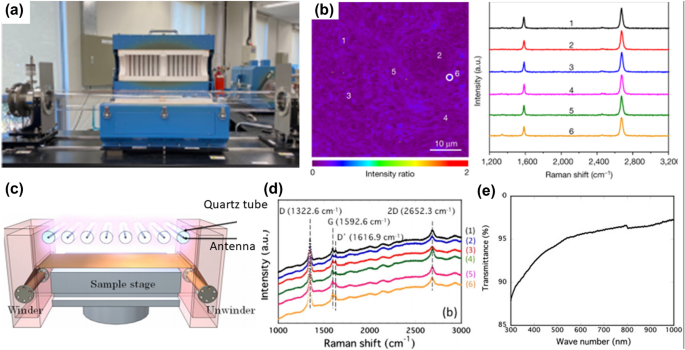
The approaches to growing high-quality graphene films on transition metal substrates are dominated by high-temperature thermal CVD. A low-temperature process for graphene synthesis would be required for applications in electronic devices, and plasma CVD could be an excellent alternative to thermal CVD. The formation of plasma from the reacting gas precursors enables thermal CVD deposition at a lower temperature. 109 Kim et al. decreased the synthesis temperature to 450 °C and reported graphene on Ni foil with the high transparency of 89%. 110 Yamada et al. used microwave plasma CVD to create 294-mm-wide FLG films on a Cu substrate at 400°C with 95% optical transmittance (Fig. 4c, d). 108 With the lowest synthesis temperature of 317°C, graphene layers having optical transmittance in the range 78–94% have been achieved. 111
Although the CVD technique has emerged as a promising method for producing large-scale graphene, the graphene layer must be transferred onto a suitable substrate for further application. In this context, thermal SiC decomposition eliminates the need for graphene transfer for synthesizing electronic devices. 112 Since the carbon vapor pressure is insignificant in comparison to that of silicon, when heated for a short period of time (1–20 min), the Si atoms desorb and leave behind the carbon atoms, which then rearrange to form graphitic layers. 113,114 Emtsev et al. have demonstrated the synthesis of large-area monolayer graphene films on SiC at normal atmospheric pressure and 1650°C. 115 The presence of argon reduces the rate of Si evaporation, resulting in a substantial enhancement in graphene surface morphology on the SiC. 116 It is also possible to synthesize wafer-scale graphene films (mm scale) at a significantly lower temperature (1100°C) on a Ni-Cu-coated SiC substrate. 117
One of the most recent techniques for producing graphene involves un-zipping of carbon nanotubes (CNT) to produce graphene nanoribbons (GNRs) in a controlled way with precise dimensions. The multiwall carbon nanotubes (MWCNTs) were unzipped by various experimental methods, such as using a mixture of acids, 118 a catalytic cutting method, 119 electric zipping, 120 and H-based unzipping, 121 etc. CNTs were utilized as the starting material for the catalytic cutting method. Carbon atoms in CNTs diffuse on the metal nanoparticles at ~ 900°C under an argon–hydrogen environment. Following that, the particles become saturated and react with H2. The cutting can be driven in one of the two directions, depending on the particle size, resulting in the armchair or zigzag edges. Elias et al. reported using Ni or Co to longitudinally cut and open MWCNTs to create graphitic nanoribbons, typically 100–500 nm long and 15–40 nm wide. 122
Similarly, Wang et al. reported the top–down synthesis of GNRs using oxidative splitting with (NH4)2S2O8 in anhydrous acidic media. 123 This method produces GNRs with a high proportion of oxygen functionalities, which alters their properties. Kumar et al. probably addressed this issue by irradiating MWCNTs with a laser pulse energy of 200–350 mJ. They demonstrated that their laser irradiation method is a simple way to produce GNRs with no surface contamination. Although CNT unzipping and subsequent trimming can effectively reduce the width of the GNR, the unzipping process has a low yield. 124
In another recent approach, Su et al. documented the synthesis of template-free nitrogen and sulfur co-doped 3D graphene networks (3DGNs) using the hydrothermal method. 125 Other than the hydrothermal method, the sugar-blowing method is currently the most fascinating and inexpensive technique for growing 3DGNs. Synthesis of a 3D graphene bubble network using the sugar-blowing approach following a polymeric predecessor was proposed by Wang et al. 126 Glucose is mixed with an ammonium salt and treated at 1350°C for 3 h under an Ar environment. A black foam-like, 3D self-supported graphene product was collected. Very recently, Han et al. also reported a sugar-blowing-assisted thermal reduction of GO to produce high-quality 3D porous graphene (3D-PG). 127 By adjusting the synthesis conditions, the microstructure and properties of the 3DGNs can control. For example, the pore size and porosity of 3D-PG can be tuned by changing the metal templates' pore structure in template-assisted CVD. Table II shows the comparison between the synthesis method, product, basic properties, and application of graphene.
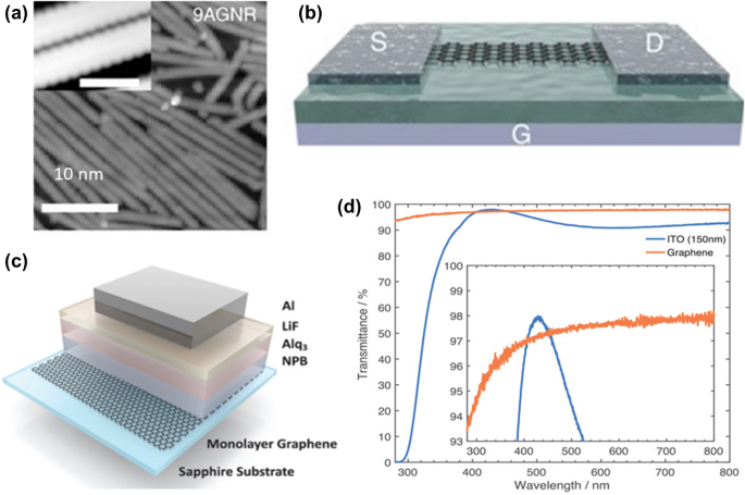
Indium tin oxide (ITO) is a transparent conducting material used in smartphones, television screens, and many touchscreen applications. However, the limited availability of indium is a growing concern in the ITO market. It is anticipated that graphene will be one of the materials that will be in the highest demand for the development of future optoelectronic devices. Gautam et al. reported 85–95% transmittance with the sheet resistance in the range of 50–350 Ω/sq for monolayer graphene to F:G. 147 Graphene-based organic light-emitting diodes fabricated directly on a transparent sapphire substrate using metal–organic chemical vapor deposition (MOCVD) is expected to have fewer defects. 130 Figure 5b, c demonstrates the schematic and optical transmittance of > 97% from the visible to the near-infrared region identical to conventional ITO anodes.
Silver films are extensively utilized as optical coatings; however, silver is expensive, unstable in air, and prone to oxidation, although common protective coatings have the ability to stop corrosion of silver, but change the optical properties. When compared to bare silver, the rate of corrosion of silver films covered with graphene was reduced by 66 times. 148 Prasai et al. 149 found that the graphene-covered copper exhibited a corrosion rate 7 times lower than that of bare copper in sodium sulfate solution. Similarly, in the case of Ni covered with graphene, an enhancement in the corrosion resistance by 20 times was obtained.
Graphene and its derivatives are also widely used as reinforcements in coatings to improve wear resistance. 150 The titanium alloy matrix has a relative wear resistance of 1 and, with an optimum graphene content of 3 g/L the resistance is increased to 12.2. Graphene-modified Al2O3/TiO2 coatings have a 20–25% lower wear rate than non-graphene coatings. 151 Zuo et al. 152 also observed an improvement in the wear resistance of a micro-arc oxidation (MAO) coating prepared on Ti-6Al-4 V alloy with GO. They found that the MAO coating with 10 mL/L GO had comparatively superior tribo-corrosion resistance, with fewer microcracks but a smoother worn surface than that of 5- and 15-mL/L GO coatings (Fig. 6a).
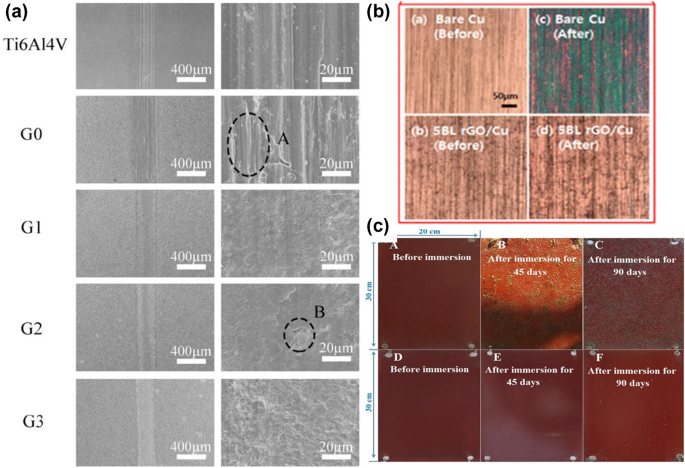
Graphene coatings can act as a high-energy barrier in the path of oxygen atoms. 155 Kang et al. 153 observed an enhancement in the oxidation resistance of Fe and Cu foils coated with rGO multilayers (Fig. 6b). Chen et al. reported similar findings, demonstrating that Cu and Si metal surfaces, when coated with graphene, are well shielded from oxidation even after being heated to 200°C for up to 4 h. 156
Superhydrophobic surfaces fabricated from graphene exhibit an excellent anticorrosion property. 154 A recent study by Miler et al. holds exciting potential for creating water-repellent coatings using gas-phase synthesized graphene, with a water contact angle of 153° ± 3°. 137 The graphene grown by their reported method immediately can repel water without any chemical modifications. In another study, the use of the matrix material PDMS and rGO produced a robust superhydrophobic surface with a water contact angle of 159° ± 2°, which had self-cleaning, antifouling, and anticorrosion properties, indicating its potential applications in the marine industry 154 (Fig. 6c).
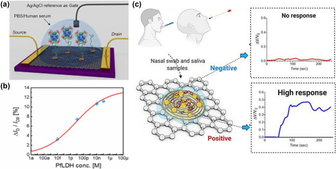
The biocompatibility of graphene derivatives allows their substantial use in medicine and biology. One of the foremost critical applications is in the early diagnosis of viruses. For example, Miranda et al. developed a graphene-based electrical biosensor for the early detection of malaria parasites (Fig. 7a, b). 157 In this study, an rGO-based field-effect transistor (2DBioFET) was biofunctionalized with molecules that selectively bind to a malaria biomarker, i.e., Plasmodium falciparum lactate dehydrogenase (PfLDH), with a detection limit down to 0.11 pg/mL. Similarly, Walters et al. developed a graphene sensor platform for rapidly diagnosing the hepatitis virus, 158 and reported a detection limit down to 100 pg/mL in less than 4 min, even with smaller volume samples, i.e., 5 μL. The sensor is easily adaptable to other infectious disease markers, such as hepatitis B virus, SARS-CoV-2, HIV, and many others. Roslon et al. developed a graphene drum to assess rapid antibiotic susceptibility to bacteria in drug screening. 159 A silicon chip containing thousands of these graphene-covered cavities was placed inside an E. coli-containing cuvette. The nanomotion of E. coli bacterium caused the suspended graphene membrane to deflect, as detected by laser interferometry, and then be converted into a soundtrack. The nano-motion of bacterium rapidly decreases in the presence of antibiotics unless the bacteria are resistant to the antibiotic.
One of the distinguishing characteristics of GO is its ability to transform stem cells into bone-generating cells known as osteoblasts. Porous 3D graphene-based scaffolds can be used for bone repair via bone tissue engineering. 161 A porous GO scaffolding was seeded with stem cells from mouse bone marrow. After 9 days, the cell number on the 3D GO scaffolds had increased by approximately 8.5-fold, which could be a new possible research direction to regenerate bone tissue.
Face masks have become a critical tool in the fight against the COVID-19 pandemic. 162,163,164,165 Huang et al. discovered that, when combined with the photothermal effect of the graphene layer, the bacterial inhibition rate could be improved by up to 80% in antibacterial masks modified with laser-induced graphene, resulting in 99.998% bacterial killing efficiency within 10 min. 166 A sensor made of a filter paper coated with graphene could detect COVID-19 in under 5 min 160 (Fig. 7c). On this sensor surface, gold nanoparticles capped with ssDNA (single-stranded nucleic acids) probes specific to the SARSCoV-2 RNA were deposited. In the presence of the SARS-CoV-2 RNA, the ssDNA hybridized with these probes. The hybridization of the viral RNA with the ssDNA sequence increases the charges at the graphene–solution interface, causing a change in the sensor's electrical response. The sensor detected a significant increase in voltage in positive samples compared to negative samples, and confirmed the presence of virus with nearly 100% accuracy. In another study, graphene coatings have been reported as a promising contender for anti-biofilm formation to prevent infection in medical implants. When the graphene layer is loaded with usnic acid (a strong antibacterial additive), the coating provides long-term anti-biofilm protection for up to 96 h. 167 The coating is highly effective against Staphylococcus aureus and S. epidermidis, two common biofilm-forming bacteria on medical implants.
Lithium-based batteries are acknowledged as one of the promising substitutes for applications in energy storage systems, due to their high energy density. One of the major reasons for the degradation in high energy density lithium-ion battery cathode materials is the formation of a dendritic structure and a solid electrolyte layer during the continuous charge–discharge cycles. Recently, Chen et al. suppressed the formation of Li dendrites using laser induced graphene combined with a porous silicon oxide coating. 168 They reported an improvement in the average coulombic efficiency to 99.3% (2.0 mAh cm −2 at 2.0 mA cm −2 ) compared to bare electrodes.
The lithium–sulfur (Li–S) battery is yet another promising candidate for next-generation rechargeable batteries. However, during the discharge cycle, the intermediate lithium polysulfide species dissociate in the electrolyte and diffuse between the cathode and anode, typically known as the shuttling effect, resulting in poor coulombic efficiency and rapidly reducing the capacity of the Li–S cells. The incorporation of a GO membrane to the sulfur cathode acted as an effective separator and reduced the cyclic capacity decay rate from 0.49% to 0.23%. 169 Laser scribed graphene, having a hierarchically 3-D porous structure, can greatly suppress polysulfide shuttling. 170 The resultant Li–S cell showed a high specific capacity of 1160 mAh/g with excellent cycling stability of 80.4% capacity retention after 100 cycles (Fig. 8a, b).
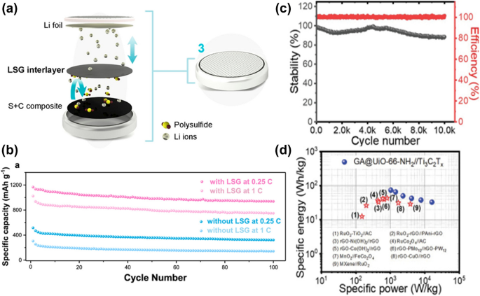
Graphene is frequently proposed as a substitute for activated carbon in supercapacitors due to its high relative surface area of 2,630 m 2 /g, which is superior for storing an electrostatic charge with almost no degradation over long-term cycling. Jayaramulu et al. created a highly efficient graphene hybrid supercapacitor by combining graphene as an electrostatic electrode and a metal–organic framework as an electrochemical electrode. The device can deliver an energy density of up to 73 Wh/kg and a power density of up to 16 kW/kg, which are comparable to Pb-acid batteries and nickel metal hydride batteries. Furthermore, standard batteries (such as lithium) have a useful life of approximately 5000 cycles. However, even after 10,000 cycles, this new hybrid graphene supercapacitor retains 88% of its capacity (Fig. 8c, d). 171
Ink-based graphene is emerging as a new technology for scalable manufacturing of printed and wearable electronics. Gaur et al. used graphene aerosol ink to print micro-supercapacitor, which showed a volumetric capacitance of 3.25 F/cm 3 at a current density of 20 mA/cm 3 with ∼80% capacitance retention after 10,000 cycles. 172 In a similar approach, Yun et al. developed graphene ink to print an extremely flexible and durable supercapacitor. 173 This micro-supercapacitor exhibited a power density of ~ 1.13 kW/kg and specific capacitance of ~ 22 F/g at a scan rate of 100 mV/s. Additionally, it is capable of being attached to power electronic devices, such as wearable skin sensors, which can be utilized for remote medical monitoring and diagnosis.
The commercialization of graphene is moving quite rapidly, with several real-world products on the horizon, and this trend is expected to accelerate in the coming years. For instance, in the sports industry, graphene is used to produce helmets, clothing, and tennis racquets. 174 Combining the mechanical and thermal benefits of graphene, an Italian-made graphene-enhanced motorcycle helmet was released in October 2016 in collaboration with the Italian Institute of Technology and the luxury design firm, Momodesign. 175 Graphene is applied as a coating to the exterior of the helmet, resulting in enhanced heat dissipation and increased user comfort. Graphene can improve the energy distribution and weight of a tennis racquet, as well as the speed and stability of the serve. 176 The tennis equipment manufacturer, Head, has already developed Graphene 360, a series of graphene-enhanced commercially available racquets. The British sportswear manufacturer, Inov-8, has produced the G-Series range of graphene-enhanced shoes as well as a pair of graphene-infused hiking boots. Utilizing graphene fibers in textiles produces antibacterial, antistatic clothing that can retain heat and block UV rays. 177 Companies such as Reebok, Direct Plus, and Versarien are already working on launching a new apparel collection that uses graphene in fabrics to help retain heat. Table III shows graphene-based products available in the market.
Table III Market availability of graphene-based productsA number of advantages of graphene, including its high surface area, chemical stability, thermal and electrical conductivities, super-hydrophobicity, flexibility, and so on have been discussed to illustrate the viability of bridging the nano-scale features of graphene to practical human-scale applications. To aid in the ongoing advancement of graphene-based materials and devices, this paper reviews the recent advances in their synthesis and applications. In terms of synthesis, various approaches have been successfully developed, indicating the feasibility of producing high-performance, high-quality, and large-area graphene. Exfoliation, chemical reduction of GO, CVD and thermal degradation of SiC, unzipping of CNTs, and other processes are among them. The CVD growth technique, among these, can generate large sheets of graphene with few or no defects and good conductivity; however, it must be taken into consideration that the quality of the material can be highly influenced by the process parameters used during the CVD growth. The exfoliation approach is compatible with industry-scale manufacturing of graphene powder, with certain methods yielding more than 50%. The qualities and performance of synthesized graphene have been demonstrated to be substantially reliant on the type of reducing agents and the synthetic process used. In terms of its practical uses, the properties of graphene have garnered much interest in a wide variety of different application domains. Graphene is commonly employed in transparent displays due to its excellent conductivity and flexibility. Because of its high sensitivity, graphene is utilized as a sensor in medical devices, particularly to detect certain viruses such as COVID-19 and malaria. Graphene is used in protective coatings for metals due to its corrosion and oxidation resistance, and, due to its high surface area and nonflammable nature, it is used as an electrode material for electrochemical energy storage devices, such as lithium batteries and supercapacitors to improve device performance when compared to those that use traditional carbon as electrode materials.
The authors acknowledge the financial support of the Science and Engineering Research Board (SERB), India (Grant No. EMR/2016/001282).